The First instruction for ORI
在CPU for MIPS系列的笔记中,我会详细介绍从一个最小的五级流水线开始不断的构建出一个完整的五级流水线(支持$MIPS ReleaseⅠ,从而将$ucos$Ⅱ进行搭载)。
ORI Instruction
下图是ORI指令的类型格式:
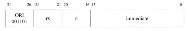
也就是说,在后续,我们需要通过001_101这一编码来判断是否是ori类型;同时,也需要注意的是:ori是I型指令,也就是有一个立即数imm。在MIPS中,imm是无符号扩展的,这一点很重要。
1 | ; ori的用法 |
A Simple Five-Stage Pipeline
在我之间的文章中,已经详细介绍过流水线(DDCA The Chapter 3 Reading, Parallelism)的概念,因此就不再赘述。本节我主要讲述的是,关于ori的完备的,简单的五级流水线系统。
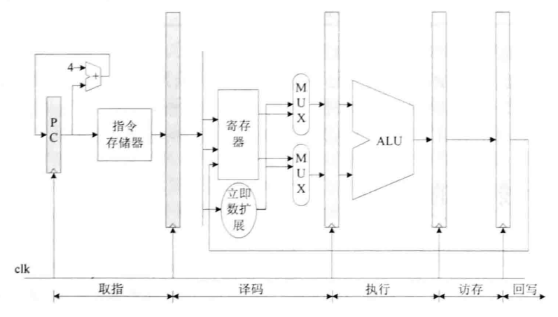
由上图可以看见,五级流水线实际上就是五个阶段过程:
- 取指
- 取指阶段是从指令存储器中取出
pc所对应的指令数据,以供译指(译码)阶段使用,而后pc自增。 - 因此,这里涉及的两个元件是
pc、inst_fetch_inst_decode和inst_rom
- 取指阶段是从指令存储器中取出
- 译码
- 译码阶段是要将从取指阶段得到的指令翻译成
cpu能够识别的二进制数据。因此,在这一阶段,我们需要对指令进行解析,比如:- 指令的类型
- 指令需要操作的寄存器(通常是读取源寄存器,写入目的寄存器)
- 指令需要操作的寄存器中的数据
- 指令中是否含有立即数
- …
- 获得如上数据后,将这些数据送往执行阶段让
cpu进行实际的执行 - 因此,这里涉及的元件有
regfile,inst_decode和inst_decode_execute
- 译码阶段是要将从取指阶段得到的指令翻译成
- 执行
- 执行阶段是根据从译码阶段得到的各种数据,进行真实的执行,比如:
- 从译码阶段获得的操作码判断操作类型,本次进行的是
ori操作,也就是或操作 - 通过从译码阶段得到的源寄存器数据和目的寄存器数据,进行或操作
- 然后指定将结果写入目的寄存器中
- 从译码阶段获得的操作码判断操作类型,本次进行的是
- 下一步便是访存阶段
- 执行阶段是根据从译码阶段得到的各种数据,进行真实的执行,比如:
- 访存
- 对于这一阶段,通常是对内存进行读写操作的指令需要进行的。因此
ori在此阶段并没有操作,将执行阶段的数据向下传递到回写阶段即可
- 对于这一阶段,通常是对内存进行读写操作的指令需要进行的。因此
- 回写
- 回写将执行的计算结果保存到目的寄存器中
因此,我们主要实现的就是一个简单的针对ori指令的五级流水线。
具体实现
上面我们已经介绍了五级流水线的基本模型,现在,就应该具体来实现每一个部分了。
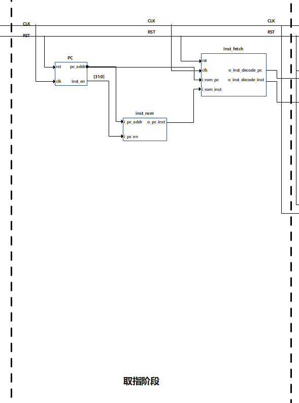
取指阶段
取指阶段要求我们根据pc从inst_rom中取出对应的指令数据,并传递给译码阶段。因此,这一阶段我们需要实现三个模块:pc、inst_rom和inst_fetch。
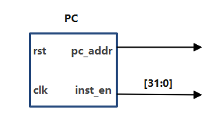
PC模块
pc的作用是给出当前指令地址,并准备下一条指令的执行。其接口对应的参数为:
| 接口名 | 宽度 | 输入/输出 | 作用 |
|---|---|---|---|
| rst | 1 | i | 复位信号 |
| clk | 1 | i | 时钟信号 |
| pc_addr | 32 | o | 要读取的指令地址 |
| inst_en | 1 | o | 指令存储器使能信号 |
1 | module pc( |
在pc模块中,我们只需要做两个极其简单的判断(在时钟上升沿时):
- 如果复位信号是开启的,那么就需要重置;反之,则给指令存储器使能信号
- 如果指令存储器使能信号没有开启,就说明
pc无法使用,则给一个初始值;反之,则需要累加4
1 | if (rst == `RST_ENABLE) ... |
注意:
为什么pc要累加4呢?因此在risc指令集中,一条指令被强制规定为4字节的,常见的有arm、mips和risc-v
此时的电路图为:
Instruction ROM模块
inst_rom的作用是存储系统中需要执行的指令,因此,该模块只与pc暂时相关联。
| 接口名 | 宽度 | 输入/输出 | 作用 |
|---|---|---|---|
| i_pc_en | 1 | i | 指令存储器使能信号 |
| i_pc_addr | 31 | i | 当前指令的地址 |
| o_pc_inst | 31 | o | 当前指令地址对应的指令 |
这里需要说明的是:
接口名的命名规范问题:
i表示输入,o表示输出
紧接着的pc就是从什么地方输入过来的信号,需要输出到哪一个模块去
最后的是信息
也就是说,接口名具体意义是(以i_pc_en为例):从pc过来的使能信号输入
1 | module rom_memory( |
在inst_rom中,我们需要做的就是创建一块内存用于保存指令数据,然后根据对应的pc地址和使能信号取出指令。因此,当前的电路为:

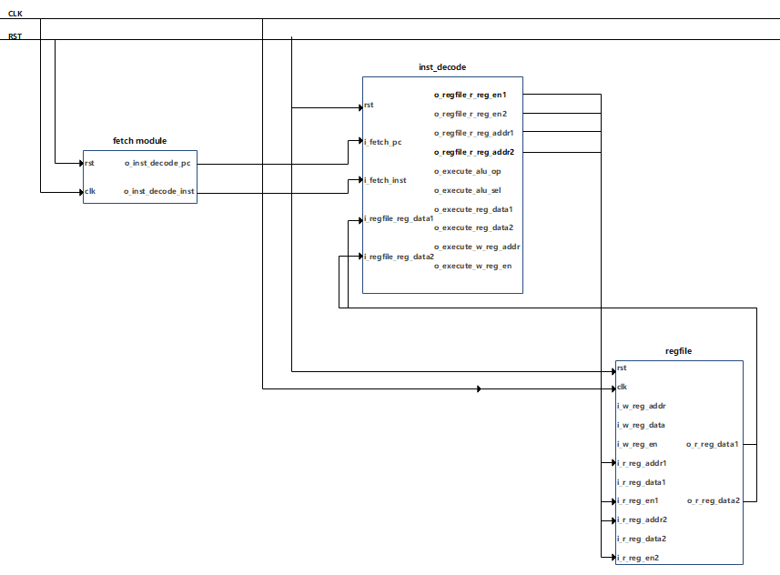
Fetch模块
inst_fetch模块的作用是暂时保存取指阶段的数据,并在下一个时钟传递给译码阶段。
| 接口名 | 宽度 | 输入/输出 | 作用 |
|---|---|---|---|
| rst | 1 | i | 复位信号 |
| clk | 1 | i | 时钟信号 |
| i_rom_pc | 32 | i | 通过pc从inst_rom模块中获得的指令地址 |
| i_rom_inst | 32 | i | 通过pc从inst_rom模块中获得的指令 |
| o_inst_decode_pc | 32 | o | 输出到译码阶段的指令地址 |
| o_inst_decode_inst | 32 | o | 输出到译码阶段的指令 |
1 | module inst_fetch( |
在inst_fetch模块中,我们不需要做任何处理,这就相当于一个中转站,将pc和inst数据发送给译码阶段的模块。
如下就是整个fetch模块的电路图:

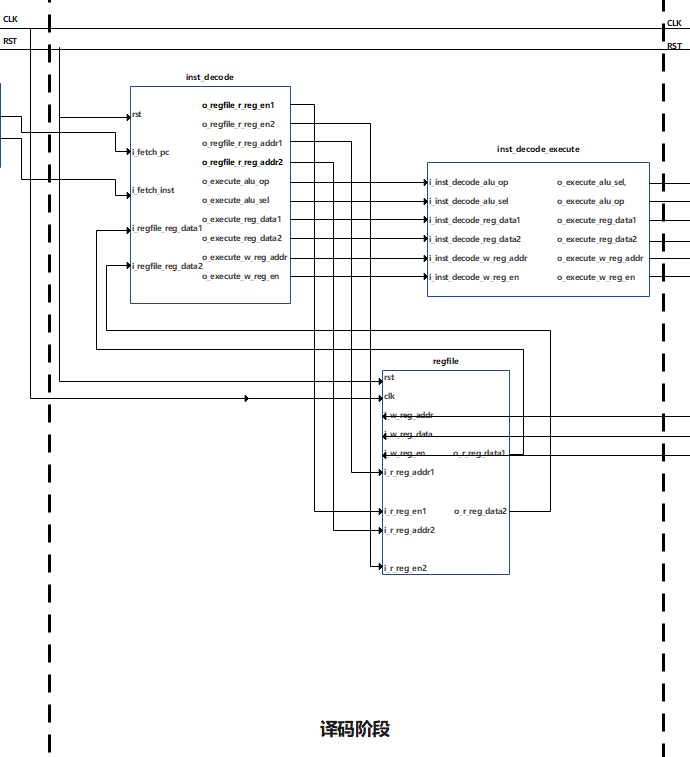
译码阶段
译码阶段需要将取指阶段的数据进行处理,然后输出到执行阶段,因此,译码阶段涉及regfile、inst_decode和inst_decode_excute模块。
Regfile模块
regfile模块主要是用于寄存器表,也就是汇编中我们使用的寄存器,其可以同时支持两个寄存器的读操作和一个寄存器的写操作。
| 接口名 | 宽度 | 输入/输出 | 作用 |
|---|---|---|---|
| rst | 1 | i | 复位信号 |
| clk | 1 | i | 时钟信号 |
| i_w_reg_addr | 5 | i | 需要写入的寄存器地址 |
| i_w_reg_data | 32 | i | 需要写入的寄存器数据 |
| i_w_reg_en | 1 | i | 写使能信号 |
| i_r_reg_addr1 | 5 | i | 第一个需要读取的寄存器地址 |
| i_r_reg_addr2 | 5 | i | 第二个需要读取的寄存器地址 |
| i_r_reg_en1 | 1 | i | 第一个读使能信号 |
| i_r_reg_en2 | 1 | i | 第二个读使能信号 |
| o_r_reg_data1 | 32 | o | 被读取的第一个寄存器数据 |
| o_r_reg_data2 | 32 | o | 被读取的第二个寄存器数据 |
1 | module regfile( |
在regfile模块中,我们需要考虑两种情况,读和写:
- 写:
- 如果
i_w_reg_en是开启的,且i_w_reg_addr不为$0,那么就将对应的i_w_reg_data写入到寄存器表中
- 如果
- 读:
- 读有四种情况:
- 第一种:如果
rs1(或rs2)需要读的寄存器为$0,那么直接赋值为0进行输出 - 第二种:如果
rs1(或rs2)需要读的寄存器刚好是写寄存器,那么直接将写寄存器的值赋值进行输出 - 第三种:如果
rs1(或rs2)单纯的读,那么将在寄存器中i_r_reg_addr对应的值赋值进行输出 - 第四种:其他情况均赋值为
0进行输出
- 第一种:如果
- 读有四种情况:
由于regfile类似于表模块,因此暂时不给出对应的电路。
inst_decode模块
inst_decode模块的作用是对指令进行译码,得到最终的运算类型、子类型、源操作数1、源操作数2和要写入的目的寄存器地址等信息。
| 接口名 | 宽度 | 输入/输出 | 作用 |
|---|---|---|---|
| rst | 1 | i | 复位信号 |
| i_fetch_pc | 32 | i | 从fetch模块中得到的pc地址 |
| i_fetch_inst | 32 | i | 从fetch模块中得到的指令 |
| i_regfile_reg_data1 | 32 | i | 从regfile模块中查询到的reg1的数据 |
| i_regfile_reg_data2 | 32 | i | 从regfile模块中查询到的reg2的数据 |
| o_regfile_r_reg_en1 | 1 | o | 输出到regfile的reg1的读使能信号 |
| o_regfile_r_reg_en2 | 1 | o | 输出到regfile的reg2的读使能信号 |
| o_regfile_r_reg_addr1 | 5 | o | 输出到regfile的reg1的地址 |
| o_regfile_r_reg_addr2 | 5 | o | 输出到regfile的reg2的地址 |
| o_execute_alu_op | 8 | o | 输出到execute阶段的指令的子类型 |
| o_execute_alu_sel | 3 | o | 输出到execute阶段的指令的类型 |
| o_execute_reg_data1 | 32 | o | 输出到execute阶段的reg1的数据 |
| o_execute_reg_data2 | 32 | o | 输出到execute阶段的reg2的数据 |
| o_execute_w_reg_addr | 5 | o | 输出到execute阶段的rd的地址 |
| o_execute_w_reg_en | 1 | o | 输出到execute阶段的rd的写使能信号 |
1 | module inst_decode( |
因此,可以看见,inst_decode会从fetch模块中得到的指令和地址进行解析,然后通过访问regfile查表操作,获得对应寄存器的操作数值作为输出;同时,在内部解析指令每一个字段含义。
1 | // 31 26 25 21 20 16 15 0 |
如上所示,第一个是ori指令的格式,而下面的是常见的R-type指令格式。因此,如果rst是关闭的,我们的初始化应该需要根据每个字段进行初始化,我们默认rs、rt和rd是存在的,也就是一般意义的R-type指令。
然后我们通过i_fetch_inst[21:26]来截取最开始的操作码,目前我们只需要判断ori指令,因此,一旦判断是ori指令后,写使能开启,指令类型是logic,子类型是or logic;又从上面可以知道ori是I-type指令,因此我们假设rt寄存器无效,rs作为第一个操作数。而imm直接由i_fetch_inst[15:0]截取后进行无符号扩展(注意,这里是大端编码),然后还需要设置rd寄存器地址,并指出该指令有效。
初始化完成后,我们就需要去regfile表中读取rs1(或rs2,如果有效的话)作为o_execute_reg_data的数据输出到execute阶段,如果rs1(或rs2)是无效的,那么对应的o_execute_reg_data就应该是imm的数据。
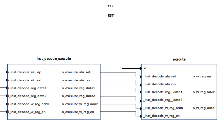
inst_decode_execute模块
这个模块和fetch模块类似,是作为inst_decode模块的输出中转站,用以在下一个时钟送往execute模块的。
| 接口名 | 宽度 | 输入/输出 | 作用 |
|---|---|---|---|
| rst | 1 | i | 复位信号 |
| clk | 1 | i | 时钟信号 |
| i_inst_decode_alu_sel | 3 | i | 从译码阶段获取的运算类型信息 |
| i_inst_decode_alu_op | 8 | i | 从译码阶段获取的子运算类型信息 |
| i_inst_decode_reg_data1 | 32 | i | 从译码阶段获取的第一个源操作数的数据 |
| i_inst_decode_reg_data2 | 32 | i | 从译码阶段获取的第二个源操作数的数据 |
| i_inst_decode_w_reg_addr | 5 | i | 从译码阶段获取的目的寄存器地址 |
| i_inst_decode_w_reg_en | 1 | i | 从译码阶段获取的目的寄存器写使能 |
| o_execute_alu_sel | 3 | o | 将要输出到execute阶段的类型信息 |
| o_execute_alu_op | 8 | o | 将要输出到execute阶段的子类型信息 |
| o_execute_reg_data1 | 32 | o | 将要输出到execute阶段的第一个操作数数据 |
| o_execute_reg_data2 | 32 | o | 将要输出到execute阶段的第二个操作数数据 |
| o_execute_w_reg_addr | 5 | o | 将要输出到execute阶段的目的寄存器地址信息 |
| o_execute_w_reg_en | 1 | o | 将要输出到execute阶段的目的寄存器写使能信息 |
1 | module inst_decode_execute( |
这里的逻辑极其简单,就是在下一个时钟上升沿时,将输入的输出转交给execute模块即可。

执行阶段
我们已经在译码阶段得到了第一个操作数数据、第二个操作数数据、指令类型、指令子类型、目的寄存器地址和目的寄存器的写使能。现在就需要通过获得的数据来进行具体的操作实现了。
execute模块
execute模块会根据译码阶段的信息,来实现对应类型的操作,然后得出应该存在目的寄存器中的数据。
| 接口名 | 宽度 | 输出/输入 | 作用 |
|---|---|---|---|
| rst | 1 | i | 复位信号 |
| i_inst_decode_alu_sel | 3 | i | 从译码阶段得到的计算子类型 |
| i_inst_decode_alu_op | 8 | i | 从译码阶段得到的计算类型 |
| i_inst_decode_reg_data1 | 32 | i | 从译码阶段得到的第一个源操作数的数据 |
| i_inst_decode_reg_data2 | 32 | i | 从译码阶段得到的第一个源操作数的数据 |
| i_inst_decode_w_reg_addr | 5 | i | 从译码阶段得到的目的寄存器地址 |
| i_inst_decode_w_reg_en | 1 | i | 从译码阶段得到的目的寄存器写使能 |
| o_w_reg_addr | 5 | o | execute模块计算后需要写入的目的寄存器地址 |
| o_w_reg_en | 1 | o | execute模块需要写入的目的寄存器的写使能 |
| o_w_reg_data | 32 | o | execute模块需要写入的目的寄存器的数据 |
1 | module execute( |
在execute模块中,我们需要根据得到的子类型来计算对应的数据,然后判断i_inst_decode_alu_sel后通过o_w_reg_data进行输出。
1 | case (i_inst_decode_alu_op) |
execute_memory模块
该模块是执行阶段和访存阶段之间的中转站,用于将execute中的输出信息转交给memory模块。
| 接口名 | 宽度 | 输入/输出 | 作用 |
|---|---|---|---|
| rst | 1 | i | 复位信号 |
| clk | 1 | i | 时钟信号 |
| i_execute_w_reg_addr | 5 | i | 从execute模块得到的目的寄存器的地址 |
| i_execute_w_reg_en | 1 | i | 从execute模块得到的目的寄存器的写使能 |
| i_execute_w_reg_data | 32 | i | 从execute中计算得到的目的寄存器的数据 |
| o_memory_w_reg_addr | 5 | o | 访存阶段将要写入的地址 |
| o_memory_w_reg_en | 1 | o | 访存阶段的使能信号 |
| o_memory_w_reg_data | 32 | o | 访存阶段将要写入的数据 |
1 | module execute_memory( |
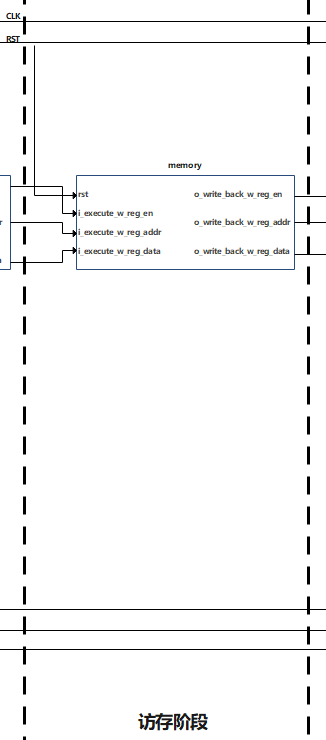
访存阶段
当执行阶段结束后,就应该进入访存阶段了,但是,ori指令并不涉及访存操作,因此我们不需要做任何事,直接将数据传给回写阶段即可。
memory模块
| 接口号 | 宽度 | 输入/输出 | 作用 |
|---|---|---|---|
| rst | 1 | i | 复位信号 |
| i_execute_w_reg_addr | 5 | i | 从执行阶段得到的目的寄存器地址 |
| i_execute_w_reg_en | 1 | i | 从执行阶段得到的目的寄存器写使能 |
| i_execute_w_reg_data | 32 | i | 从执行阶段得到的目的寄存器数据 |
| o_write_back_w_reg_addr | 5 | o | 输出到写回阶段的目的寄存器的地址 |
| o_write_back_w_reg_en | 1 | o | 输出到写回阶段的目的寄存器的写使能信号 |
| o_write_back_w_reg_data | 32 | o | 输出到写回阶段的目的寄存器的值 |
在ori中,没有任何操作。
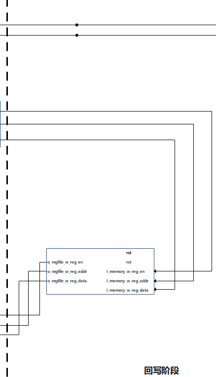
回写阶段
回写阶段实际上是两部分组成,一个是memory_write_back模块,一个就是通过该模块回写到regfile中。
memory write back模块
| 接口名 | 宽度 | 输入/输出 | 作用 |
|---|---|---|---|
| rst | 1 | i | 复位信号 |
| clk | 1 | i | 时钟信号 |
| i_memory_w_reg_addr | 5 | i | 从访存阶段得到的目的寄存器地址 |
| i_memory_w_reg_en | 1 | i | 从访存阶段得到的目的寄存器写使能 |
| i_memory_w_reg_data | 32 | i | 从访存阶段得到的目的寄存器数据 |
| o_regfile_w_reg_addr | 5 | o | 回写到regfile模块的目的寄存器地址 |
| o_regfile_w_reg_en | 1 | o | 回写到regfile模块的目的寄存器写使能 |
| o_regfile_w_reg_data | 32 | o | 回写到regfile模块的目的寄存器数据 |
1 | module memory_write_back( |
顶层模块构建
目前,我们已经完成了ori的五级流水线的五个部分,现在就应该通过顶层模块来布线了。
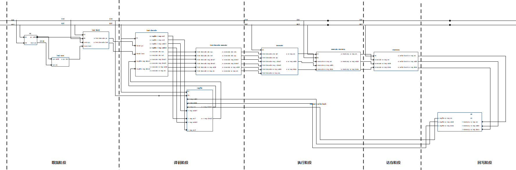
每一个部分分别为:

最终我们得到如下电路图:

……世纪长图